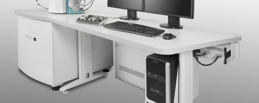
Imaging of topographical features and chemical phase differences, with elemental analysis
SEM-EDX can be used to provide surface elemental composition information of areas as small as nanometers in diameter. A finely tuned electron beam scans the sample and monitors the reflected electrons from the sample surface. The impact of the electron beam produces x-rays that are characteristic of the elements in the sample. SEM-EDX is also capable of analyzing multiple spots to create elemental maps of the surface of a sample, which can indicate materials present in either broad phases, or as small localized impurities. SEM-EDX detects all the elements from B to U, with detection limits of 1000 – 3000 ppm, depth resolution of 0.5-3um, and a probe size of 15-45 Å.
- Identification of surface elemental composition
- Thin films analysis
- Examination of surface morphology
- Particle contamination identification
- Identification of trace impurity spots


